
Process
PROCESS
- Prepare both front end tooling traveler and production traveler detailing all instructions necessary to manufacture the board, using customer supplied data. Review all customer documents and resolve all manufacturing issues with customer through engineering query.
- Create photo printing masters (photo tools) from the plotted silver films. Punch tooling holes into the film and certify all photo tools
- Create photo printing masters (photo tools) from the plotted silver films. Punch tooling holes into the film and certify all photo tools
- Create photo printing masters (photo tools) from the plotted silver films. Punch tooling holes into the film and certify all photo tools
- Create photo printing masters (photo tools) from the plotted silver films. Punch tooling holes into the film and certify all photo tools
- Create photo printing masters (photo tools) from the plotted silver films. Punch tooling holes into the film and certify all photo tools
- Create photo printing masters (photo tools) from the plotted silver films. Punch tooling holes into the film and certify all photo tools
- Create and certify master drill used to for all holes on the production panel
- Coat each inner layer with a photo resist material and transfer the circuit board image using photo tool artwork. Then develop the photo image. Etch the unwanted copper, leaving isolated conductors in the circuit pattern then strip the remaining photo resist.
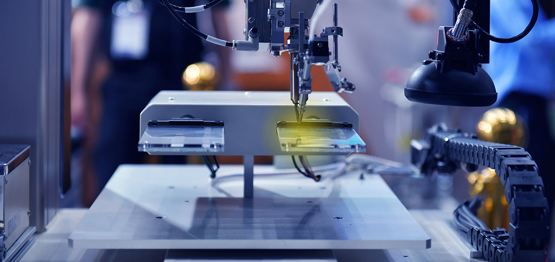
- Inspect all layers using Automated Optical Inspection (AOI) system for quality and conformance to customer specifications.
- Clean copper circuitry and apply an oxide treatment to enhance bonding during lamination process and ensure no delamination occurs.
- Stack or book inner layers and press together to form one composite, multilayer panel.
- Drill holes through board to establish a continuous path between layers and to provide holes for customers to mount any through hole components.
- Dip panel in an electroless copper solution which will deposit a thin layer of copper in the barrel of the drilled holes. This is the beginning of the plating process.
- Coat the panel with a photo resist material,transfer the outer layer circuit board images to the panel using top & bottom phototool artwork, then develop the photo image.
- Electroplate panels In a copper solution to form electrical conductors on circuits and in holes that require plating. Coat the holes and circuitry with tin coating to protect them during the etching process.
- Remove photo resist to expose the base copper. Etch away the unwanted copper, leaving the customer designed circuit pattern.
- Electrically test the panel for opens and shorts, using a custom designed bed of nails to test conductivity. Or for smaller orders a Flying Probe Tester can be utilized that is fixtureless and incorporates multiple probes to test the board by simultaneously probing a consolidation of nets predetermined by its software. Coat the circuit pattern with a solder resist ink and print a legend (or silkscreen) onto the panel to identify various component locations.
- The following four (4) processes, 15-15c, offer the customer a choice of surface finishes. The first is HASL, or Hot-Air-Solder- Level. This process involves dipping the panel in molten solder, then running the panel through air knifes that to even out the solder coating on the board surface and blow the solder from the plated through holes.
- Immersion silver: Process panels through a series of successive baths first to preclean, then to activate the copper before applying an immersion silver surface finish that has become increasingly popular for today’s fine pitch SMT devices including BGA and uBGA’s. Surface coplanarity between the SMT devices and the PWB footprint is achieved to facilitate assembly.
- Electroless Nickel/Immersion Gold: Process panels through a series of successive baths first to preclean, then to activate the copper before applying an ENIG surface finish that has become increasingly popular for today’s fine pitch SMT devices including BGA and uBGA’s. Surface coplanarity between the SMT devices and the PWB footprint is achieved to facilitate assembly.
- Organic Solderability Preservative (OSP): Process panels through a series of successive baths first to preclean, then to activate the copper before applying an OSP surface finish that has become increasingly popular for today’s fine pitch SMT devices including BGA and uBGA’s. Surface coplanarity between the SMT devices and the PWB footprint is achieved to facilitate assembly.
- Micro-sections are taken from a coupon or board from each lot, then potted and polished before being examined for through hole integrity as it pertains to copper thickness and uniformity and interconnect integrity. This data will be part of the first article report if required.
- Cut the individual circuit boards out of the panel with a CNC machine. This process also includes the possibility of scoring the boards within an array for dismemberment after delivery and assembly.
- Electrical test, dimension and visual inspection, and quality audit ensure compliance with customer requirements.
- Package, label and ship the finished circuit boards according to the customer’s specifications.